Ever stared at a tangled mess of wires on your DIY projects and thought, "There must be a better way"? I certainly have. Transforming my projects from a jumble of wires to sleek, professional-looking devices seemed daunting at first. But guess what? Making a custom DIY PCB (Printed Circuit Board) is easier than you might think. In this guide, I'll share how I made my first PCB in just 10 minutes, and how you can do it too.
Why I Decided to Create a PCB
Understanding the motivation behind a project can make all the difference. Here's why I took the plunge into PCB creation.
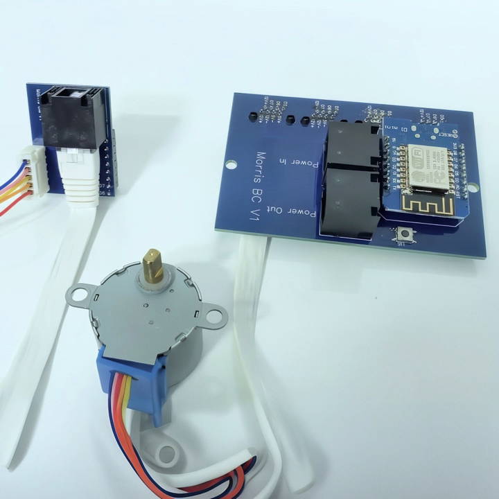
From Messy Wires to Professional Boards
No matter how simple a project is, if it looks like a bird's nest of wires, it's hard to convince others (or even yourself) that it's reliable or safe. I've had people look at my DIY setups and say:
- "That seems too complicated!"
- "Isn't that a fire hazard?"
Even though my projects were safe and functional, their DIY appearance didn't inspire confidence. I wanted a cleaner, more professional look.
Challenges with DIY Projects
People often suggest that I should make and sell my projects. However, there are three big hurdles:
- Handling Returns and Warranties: Dealing with potential returns and warranty claims is a headache I wanted to avoid.
- Fair Compensation: If I charged fairly for my time and effort, the cost wouldn't be attractive to buyers.
- DIY Aesthetics: Homemade projects, no matter how well they work, often lack the polished look that appeals to consumers.
Creating a PCB addressed the third point, giving my projects a professional appearance without the commercial production hassles.
Understanding PCBs: The Basics
Before diving in, I needed to grasp what a PCB actually is.
What Exactly Is a PCB?
A Printed Circuit Board (PCB) is a board made from a non-conductive material that supports and connects electronic components using conductive pathways, known as traces. Essentially, it's a platform that organizes your components and connections in a neat, reliable manner.
Key Components of a PCB
Learn about the key components of a pcb, including surface mount vs. through-hole components, solder mask, traces, and ground planes.
Surface Mount vs. Through-Hole Components
- Surface Mount Technology (SMT): Components are placed directly onto the surface of the PCB. This method allows for smaller components and more compact designs but can be trickier for beginners to solder.
- Through-Hole Technology (THT): Components have leads that go through holes in the PCB and are soldered on the opposite side. This method is more forgiving and easier for novices.
For my first PCB, I chose through-hole components to keep things simple.
Solder Mask
- What Is It?: A thin lacquer-like layer applied over the copper traces.
- Purpose: It prevents solder from bridging between conductors, reducing the chance of shorts. Plus, it gives the PCB its characteristic green (or other colored) finish.
Traces and Ground Planes
- Traces: The copper pathways that connect components, acting like wires.
- Ground Plane: A large area of copper connected to the ground terminal of the circuit. It helps reduce electrical noise and assists with heat dissipation.
Step by Step Instructions
Learn how to make your own DIY circuit board with this step-by-step guide. Follow easy instructions from planning to testing for successful results.
Step 1: Planning and Gathering Materials
Planning and gathering materials for your project? Learn how to choose the right project and find essential components easily.
Choosing the Project
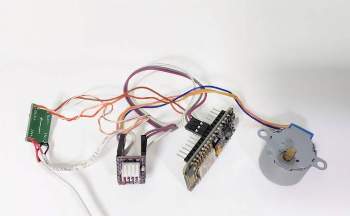
I decided to create a PCB for my window blinds automation project. The goal was to replace the messy wiring with a clean, professional-looking board.
Components Needed
- ESP8266 NodeMCU: The microcontroller that serves as the brain of the project.
- Buck Converter: To step down voltage to the required level.
- Screw Terminals: For secure and removable power connections.
- Ethernet Jacks: To connect multiple blinds using standard cables.
Tip: When gathering components, having the exact part numbers helps in finding accurate representations in PCB design software.
Step 2: Getting Familiar with EasyEDA
Discover why I chose EasyEDA and learn how to set up your project with this comprehensive guide. Perfect for beginners looking to get familiar with EasyEDA.
Why I Chose EasyEDA
- Free and Online: No need to install software; accessible from any browser.
- Extensive Component Library: Simplifies finding and adding parts.
- User-Friendly Interface: Ideal for beginners.
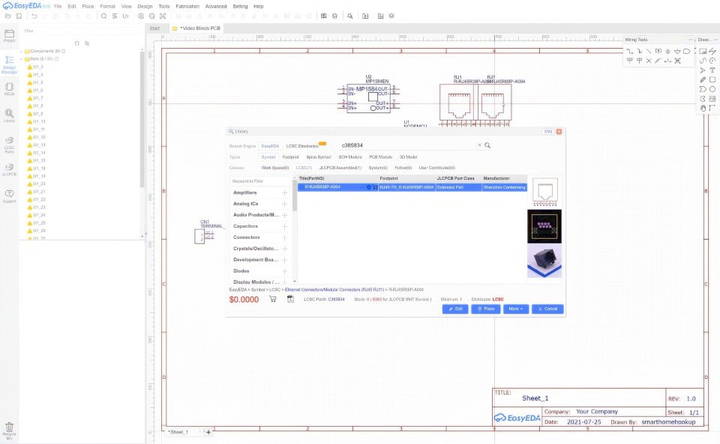
Setting Up the Project
- Creating an Account: I used my Google account for quick access.
- Starting a New Project: Named it "Blinds Automation PCB" for easy reference.
Tip: Organizing your projects with clear names helps when you have multiple designs.
Step 3: Designing the Schematic
Master the art of designing schematics, adding components, and connecting them seamlessly in one comprehensive guide. Perfect for all skill levels!
Adding Components to the Canvas
- Using the Search Function: I found components by entering their part numbers or descriptions.
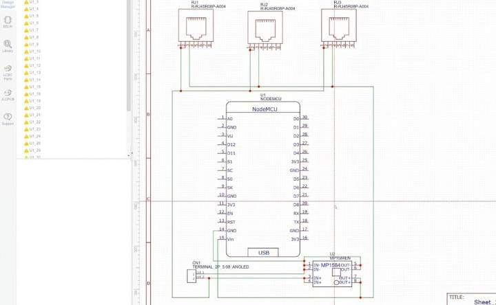
- Placing Components: Dragged each onto the schematic canvas, arranging them logically.
Connecting the Components
- Drawing Connections: Used wires to connect pins according to my project's needs.
- Labeling Nets: Assigned names like VCC (positive voltage) and GND (ground) to keep track of connections.
Tip: Keeping your schematic organized makes troubleshooting and future revisions much easier.
Step 4: Converting to PCB Layout
Learn the essentials of converting to pcb layout, transitioning to pcb design, placing components, and adding silkscreen labels efficiently.
Transitioning to PCB Design
- Converting the Schematic: Used the "Convert to PCB" function.
- Addressing Warnings: Ignored warnings about unconnected nets for unused pins.
Placing Components on the PCB
- Component Placement: Arranged components to reflect the physical layout I desired.
- Layer Selection: Assigned components to either the top or bottom layer, depending on their placement.
Adding Silkscreen Labels
- Text and Graphics: Added labels for ports, pins, and instructions.
- Layer Selection for Labels: Used the silkscreen layer so the text would be printed on the board.
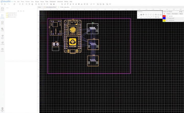
Tip: Clear labeling on the PCB helps during assembly and any future troubleshooting.
Step 5: Routing the Traces
Effortlessly master routing the traces in EasyEDA. Learn the importance, use the auto router feature, and review adjustments.
Understanding the Importance of Routing
Proper routing ensures that electrical signals travel efficiently between components without interference or unintended connections.
Using Auto Router in EasyEDA
- Accessing the Auto Router: Found under the "Route" menu.
- Setting Design Rules: Created specific rules for traces carrying higher current, like power lines, to be wider.
- Running the Auto Router: Let the software automatically connect the nets.
Reviewing and Adjusting
- Manual Adjustments: Fine-tuned any traces that seemed inefficient or messy.
- Layer Optimization: Ensured that traces on different layers didn't interfere.
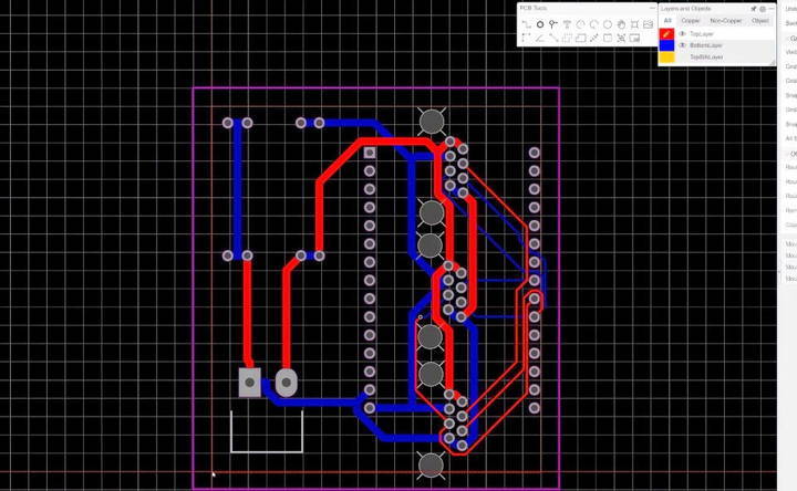
Tip: While auto-routing is convenient, manual adjustments can often optimize performance and aesthetics.
Step 6: Finalizing the PCB
Ensure your pcb design is flawless by double-checking everything and generating accurate gerber files for finalization.
Double-Checking Everything
- Layer Review: Examined each layer individually for errors.
- Design Rule Check (DRC): Ran a check to catch any issues before manufacturing.
Generating Gerber Files
- What Are Gerber Files?: Standard file format for PCB designs used by manufacturers.
- Generating Files: Used EasyEDA's built-in function to create the files needed.
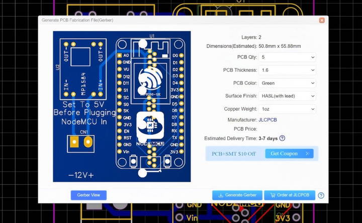
Tip: Always keep a backup of your Gerber files in case you need to reorder or make revisions.
Step 7: Ordering the PCB
Effortlessly order your pcb by choosing a manufacturer, uploading your design, and placing your order for high-quality printed circuit boards.
Choosing a Manufacturer
I opted for PCBWay due to their competitive pricing and positive reviews.
Uploading and Ordering
- Entering Specifications: Input board dimensions, layers, and other preferences.
- Uploading Gerber Files: Submitted my design for review.
- Selecting Shipping Options: Chose a balance between cost and delivery time.
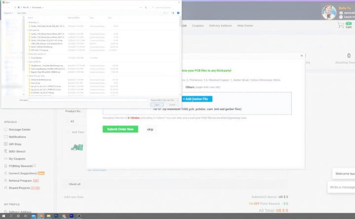
Tip: Consider the production and shipping times when planning your project timeline.
Step 8: Assembling the PCB
A complete guide on assembling the pcb, from receiving pcbs to preparing, soldering techniques, and using header pins. Perfect for electronics enthusiasts!
Receiving the PCBs
When the boards arrived, I was thrilled to see my design come to life. The professional finish added a level of satisfaction that messy wires could never provide.
Preparing to Solder
- Gathering Tools: Soldering iron, solder, flux, and safety gear.
- Organizing Components: Laid out all parts in the order they would be soldered.
Soldering Techniques
- Through-Hole Soldering Tips:
- Heat both the pad and the component lead.
- Apply solder to the joint, not the iron.
- Avoiding Common Mistakes:
- Don't overheat components.
- Use flux to improve solder flow.
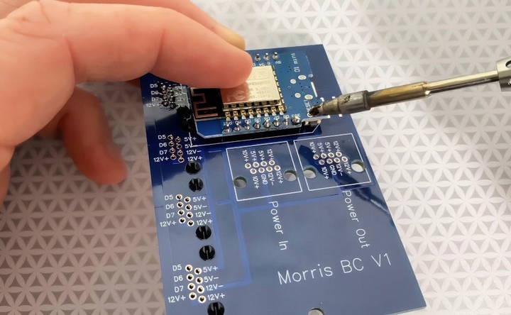
Tip: Practice on a spare board if you're new to soldering to build confidence.
Using Header Pins
I chose to use female header pins for certain components, like the NodeMCU, allowing for easy removal or replacement.
Step 9: Testing the Completed PCB
Discover how to expertly perform an initial power-up and verify functionality when testing the completed pcb for optimal performance.
Initial Power-Up
- Safety First: Checked for any visible shorts or misalignments.
- Gradual Power Application: Used a current-limited power supply for the first test.
Verifying Functionality
- Connectivity Tests: Ensured all ports and connections worked as intended.
- Operational Tests: Ran the automation script to control the blinds.
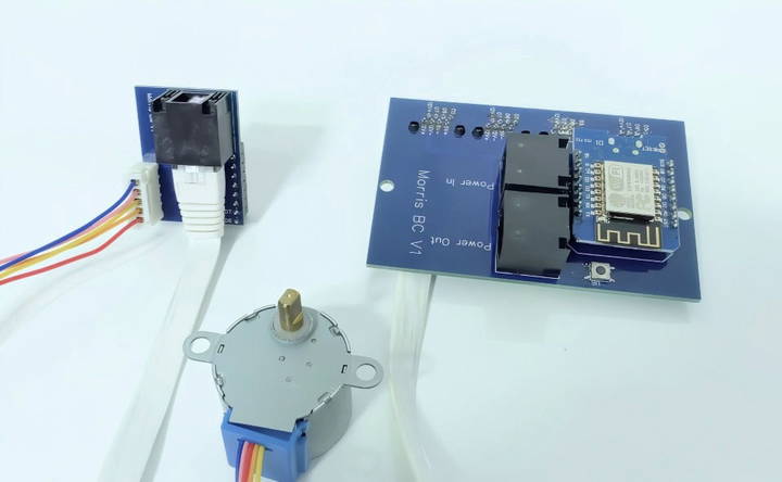
Tip: If something doesn't work, retrace your steps from the schematic to the physical connections.
Reflecting on the Experience
Making my first PCB was more than just assembling a board; it was a journey of learning and personal growth.
Benefits I Noticed
- Professional Appearance: The project looked like a commercial product.
- Simplified Wiring: Reduced the chances of errors and made troubleshooting easier.
- Reproducibility: I can now produce multiple copies with minimal effort.
Challenges Faced
- Learning Curve: Getting familiar with the design software took time.
- Patience Required: Waiting for the boards to arrive tested my eagerness.
Tips for Fellow Beginners
If you're considering creating your own PCB, here are some insights from my experience.
Start Simple
Begin with a straightforward project to understand the basics before tackling complex designs.
Utilize Resources
- Online Tutorials: There are countless guides and videos available.
- Community Forums: Places like Reddit or Stack Exchange can offer valuable advice.
Don't Rush the Design
Take your time during the schematic and PCB layout stages to minimize errors.
Practice Soldering
Good soldering skills make assembly smoother and reduce the risk of damaging components.
Exploring Advanced PCB Concepts
Having successfully created a basic PCB, I'm excited to delve into more complex aspects.
Surface Mount Technology (SMT)
- Advantages: Smaller components, more compact designs.
- Challenges: Requires precision and often specialized equipment.
Multi-Layer PCBs
- More Layers, More Complexity: Useful for intricate circuits where space is limited.
- Considerations: Increased cost and design complexity.
Custom Circuit Design
Moving beyond connecting pre-made modules to designing custom circuits for specific functions.
Conclusion
Start making on PCB creation was a rewarding endeavor that elevated both my projects and my understanding of electronics. The transformation from a cluttered breadboard to a sleek, professional PCB is incredibly satisfying.
Leveling Up Your DIY Skills: Advanced Techniques
Boost your DIY skills with advanced techniques for SMDs, double-sided, multilayer, and flexible PCBs, plus custom enclosures for expert-level projects.
1. Surface Mount Devices (SMDs)
If you're ready to take on smaller, more complex projects, it's time to explore the world of SMDs. These tiny components are mounted directly onto the surface of the board, saving space and allowing for more intricate designs. Working with SMDs requires a bit more finesse and specialized tools like a fine-tipped soldering iron and tweezers, but it opens up a whole new realm of possibilities for your DIY electronics.
2. Double-Sided PCBs
Double-sided PCBs offer more real estate for your components and traces, enabling you to create more compact and sophisticated circuits. Etching both sides of the board requires careful alignment and planning, but the results can be impressive.
3. Multilayer PCBs
For even greater complexity and density, multilayer PCBs take it to the next level. These boards consist of multiple layers of conductive material sandwiched together, allowing for intricate routing and better signal integrity. Multilayer PCBs are typically manufactured professionally, but understanding the concept can inspire future projects.
4. Flexible PCBs
Flexible PCBs, also known as flex circuits, are bendable and can conform to various shapes, making them ideal for applications where space is limited or movement is required. Working with flexible materials requires different handling techniques, but it adds a new dimension of versatility to your DIY capabilities.
5. Custom Enclosures
Once your circuit is complete, protect and showcase it with a custom enclosure. Design and fabricate a housing that fits your board perfectly, using materials like acrylic, wood, or 3D-printed plastic. A well-crafted enclosure not only adds a professional touch but also safeguards your electronics from the elements.
Remember:
- These advanced techniques may require additional tools, materials, and skills.
- Start with simpler projects and gradually work your way up to more complex designs.
- There are plenty of online tutorials and resources available to guide you through the learning process.
- Don't be afraid to experiment and explore new possibilities!
With practice and perseverance, you can master these advanced techniques and create truly remarkable DIY electronics.
Troubleshooting: Don't Let Setbacks Slow You Down
Even with the best planning, DIY circuit boards can throw a curveball or two. But don't worry! Here are some common hiccups you might encounter and how to get back on track:
1. Etching Problems:
- Uneven etching or no etching at all: Your etchant solution might be too old, too cold, or not agitated enough. Check its freshness, warm it up a bit (carefully!), and keep it moving. Also, double-check your resist for any breaks or scratches that might be letting the etchant through where it shouldn't.
2. Soldering Issues:
- Solder bridges: These unwanted connections between components happen when solder flows where it's not supposed to. A fine-tipped soldering iron and a bit of flux can help you avoid them. If they do occur, carefully remove excess solder with desoldering braid or a solder sucker.
- Cold solder joints: These weak connections look dull and grainy. Reheat the joint with your iron until the solder melts and flows smoothly, creating a shiny, concave surface.
3. Circuit Malfunctions:
- Circuit doesn't work as expected: This can be frustrating, but don't panic! Start by double-checking your circuit design and component placement. Ensure all components are correctly oriented (watch out for those pesky polarized ones!). Use a multimeter to test for continuity and identify any shorts or open circuits.
Remember:
- Patience is key! Troubleshooting takes time and a methodical approach.
- Don't be afraid to ask for help. Online forums and communities are full of helpful folks who've likely encountered similar issues.
- Learn from your mistakes. Each challenge you overcome adds to your DIY expertise.
With a little persistence and these troubleshooting tips, you'll be back to building awesome circuits in no time.
Safety First: Protect Yourself While Building
DIY electronics can be a lot of fun, but it's important to keep safety in mind. Here are some key precautions to take:
Chemical Safety
- Etching chemicals: These solutions can be corrosive and irritate your skin and eyes. Always wear gloves and safety glasses when handling them. Make sure to work in a well-ventilated area to avoid inhaling fumes.
- Solder and flux: While not as harsh as etchants, solder and flux can also cause skin irritation. Wash your hands thoroughly after using them.
Electrical Safety
- Unplug before you tinker: Always disconnect your circuit from any power source before making changes or adjustments. This prevents accidental shocks.
- Respect high voltages: If your project involves higher voltages (above 50V), take extra precautions and consult resources on working safely with electricity.
- Watch for heat: Soldering irons get very hot! Be careful not to touch the tip and avoid leaving the iron unattended when plugged in.
General Workshop Safety
- Keep it tidy: A cluttered workspace increases the risk of accidents. Organize your tools and materials and keep walkways clear.
- Proper ventilation: Ensure good airflow, especially when working with chemicals or solder fumes.
- Fire safety: Have a fire extinguisher readily available and know how to use it.
Remember:
- Read and follow all safety instructions provided with your tools and materials.
- If you're unsure about anything, ask for help from a knowledgeable person or consult online resources.
- Safety is paramount! Don't take shortcuts that could put you at risk.
By taking these simple precautions, you can enjoy your DIY electronics projects safely and confidently.
FAQs About DIY Circuit Board
Discover answers to all your FAQs about DIY circuit boards. Learn about design, assembly, components, and troubleshooting in one place.
If you can't access traditional etching chemicals, consider these alternatives:
Laser printing and ironing: Print your circuit design onto glossy paper using a laser printer and then transfer it to the copper board using heat from an iron.
CNC milling: A CNC machine can precisely mill away unwanted copper, leaving your circuit design intact. This method offers greater precision and repeatability but requires specialized equipment.
Vinyl cutting: Use a vinyl cutter to create a stencil of your circuit design, then apply it to the copper board and etch as usual.
For finer traces, use a photoresist method instead of toner transfer. Photoresist offers better resolution and allows you to create intricate patterns. Alternatively, use a permanent marker with a fine tip to draw your circuit directly onto the copper board.
Make sure your soldering iron tip is clean and properly tinned. Use flux to help the solder flow smoothly and adhere to both the component leads and the copper pads. If necessary, use a small amount of hot glue or double-sided tape to temporarily secure components in place before soldering.
Yes, you can reuse the etching solution until it becomes saturated with copper and loses its effectiveness. You can tell it's time to replace the solution when it takes significantly longer to etch a board or the etching is uneven.
Numerous websites and online communities offer tutorials, project ideas, and troubleshooting tips for DIY circuit board enthusiasts. Check out Instructables, Adafruit Learning System, SparkFun tutorials, and relevant subreddits like r/electronics and r/diyelectronics.
Final Thoughts
Don't let intimidation hold you back from trying PCB design. With accessible tools like EasyEDA and supportive communities, creating your own DIY PCB is within reach.
Have you created your own PCB or are you planning to? I'd love to hear about your experiences and any tips you might have. Let's continue learning and innovating together!
By sharing my journey, I hope to inspire you to take your DIY projects to the next level. Remember, every expert was once a beginner.


